In 1965, Gordon Moore, co-founder of Intel, wrote that semiconductor manufacturers were doubling the number of components inside integrated circuits with every successive generation. This astute prediction, later dubbed Moore’s Law, has guided the semiconductor industry for more than 50 years. As semiconductors have gotten smaller, it’s imposed even greater challenges on the design and operations cleanrooms in semiconductor factories. We take a look at how to manage these challenges and keep your wafer fab cleanroom operations running smoothly.

To learn more about the wafer fab cleanroom challenges facing semiconductor manufacturers, we spoke with Mark Burgholzer, whose career includes 22 years of hands-on experience working as an Equipment Engineer at the former Sharp Labs of America fab plant in Camas, Washington.
We asked Mark if he could share some of his practical experience working in the semiconductor manufacturing industry — especially the ins and outs of how to design cleanrooms — as well as gathering tips from him on how to keep everything running smoothly from a maintenance perspective.
Cleanroom Contamination Threat Grows as Semiconductor Components Shrink
First off, we wanted to get an idea about the relative size of the miniature components inside modern integrated circuits. Just how small are they?
(SPOILER ALERT: The answer is very small.)

Mark started by explaining that the diameter of a human hair is between 17,000 and 181,000 nanometers. The smallest known bacterium is about 400 nanometers in diameter. Human viruses are even smaller, with diameters ranging between 20 and 400 nanometers (The length of some big filoviruses can stretch to a whopping 1400 nanometers.)

Next Mark gave us a pop quiz. Could we guess the size of individual circuit components inside each of these popular consumer products?
- Apple iPhone 6S
- Xbox One S
- Nvidia GeForce Series 10 GPU
Are the circuit components used in these popular consumer products bigger or smaller than a human virus?
The answer is smaller. Each one of those products is built around computer processors whose individual components measure somewhere between 14 and 16 nanometers.
Mark pointed out that shrinking circuit sizes can make the job of semiconductor manufacturers much more difficult. Small particles floating in the air — from dust to suspended powders, emulsions, and other aerosols — can interfere with the delicate process of passing light through a photomask of the circuit design to “print” it into silicon. That’s why so much effort goes into creating a highly effective cleanroom to keep unwanted particles away from the manufacturing process.
Before diving into our main topic, designing and maintaining cleanrooms, we needed to understand more details about the circuit printing process. Mark explained that the method for creating semiconductors on a chip is actually a form of print lithography — a straightforward process in theory, but one that requires many precise steps.
In brief, crystalline silicon wafers are spin-coated with a thin layer of photo-resist material. The desired circuit design layout is printed onto a photomask, which is mounted inside a hermetically-sealed frame, known as a reticle.
Unlike regular film photography that uses a negative image to create a photograph, the photomask used in semiconductor manufacturing is a positive image (the opaque lines on the mask represent the circuit wires; the transparent areas signify the voids). Thus, when the light is projected through the photomask, it optically “prints” a negative image of the circuit design onto the wafer, creating a chemical reaction in the photo-resist material in the void areas. (The photo-resist material where the wires belong is unaffected.)
This printing process gets repeated multiple times – to fit as many circuit designs onto the disk-shaped silicon wafer as possible. In approach, the “scanner” method, the reticle (holding the photomask) and the wafer are moved in front of a mirror that projects multiple copies of the circuit design onto the wafer. In the “stepper” method, micro-stepper motors move the wafer relative to the reticle, stopping at each point to make additional exposures.
Once the whole wafer disk is “printed,” the areas of photo-resist material that were exposed to light can be removed using a chemical process, allowing the final design to be etched into the wafer using an acid bath wash.
Got it? As you can see it’s quite an involved process that only a few semiconductor fabrication plants (or fabs) around the world are capable of doing.
Is a Semiconductor Cleanroom Considered a Tech Lab or a Wet Lab?
Now that we have a basic understanding of the processes needed to etch integrated circuit designs into a silicon wafer, we wanted Mark to share his experiences with managing cleanrooms setups at Sharp Labs.
(In a previous Formaspace article, 12 Tips for Lab Architects Designing Cleanrooms, we shared research on some of the critical factors that designers need to know when planning new cleanroom facilities. Check out our report here.)
Our first question to Mark is whether he considered the cleanrooms used in semiconductor manufacturing to fall into the Tech Lab or Wet Lab category.
As you may know, in a cleanroom designed for a Tech Lab, the goal is to protect the product from human interaction, from accidental fingerprints to other forms of contamination. In contrast, the primary design objective when creating a Wet Lab cleanroom is to protect the human workers from chemicals or fumes, using safety features such as fume hoods, etc.
Mark explained that in semiconductor fab cleanrooms, workers work at wet benches equipped with powerful exhaust systems – so, from that standpoint, they would fall into the Wet Lab cleanroom category. However, cleanrooms at semiconductor manufacturers can also be considered part of the Tech Lab category, due to their use of ESD grounding straps, which we’ll touch on later.
How to Design Cleanroom Layouts to Optimize Air Flow
According to Mark, the secret to smooth operations in a semiconductor cleanroom facility is to keep that air moving, 24 x7.
In a semiconductor fab cleanroom, air is blown from the ceiling down to the floor, creating a constant, uniform stream of air, known as Vertical Laminar Flow. When the air reaches the raised platform floor, it exits through small perforated holes; it then passes upward through the air plenum to be purified through HEPA filters. The return air is also conditioned to control its temperature and humidity (this also reduces the concentration of contaminants suspended in the air) before it’s cycled through the cleanroom again.
Next, we wanted to know additional specifics about the layouts for cleanrooms used in semiconductor manufacturing. For example, what could Mark tell us about the furniture layouts and equipment setups?
According to Mark, the underlying design principle is to avoid interrupting the vertical laminar air flow that moves from the ceiling to the floor. With this principle in mind, it’s considered good practice to position any furniture or equipment along the outer walls to avoid blocking the center areas where maximum airflow occurs.
In fact, the wet bench areas where workers manipulate the wafers are inset within the exterior walls of the cleanroom. High-power exhausts built into these wet bench work areas extract the chemical vapors generated during the manufacturing process — without disrupting the air movement in the center of the room.
Next, we asked about any storage furniture or mobile carts used inside cleanroom facilities at semiconductor manufacturing facilities.
Mark explained that, in his experience, they used wire racks and wire shelves rather than use solid surfaces for storage. Mobile carts used in the cleanroom were made of wire rack materials as well – all in the interest of maximizing the airflow and eliminating flat surfaces where particles could collect.
Wall surfaces in the cleanroom use a special design as well – a honeycomb structure sandwiched between two sheets of aluminum. These walls are quite thin, only 3/8 of an inch or so, so they’re not structural (a large external frame outside the clean room supports the heavy over HVAC and air filtering equipment), but using smooth aluminum wall surfaces helps keep the air moving.
Procedures to Recover from Contamination Events in a Semiconductor Cleanroom
We also wanted to know, what can go wrong in a cleanroom?
Mark explained that the top priority is to avoid air handling shutdowns if at all possible because that’s when the contamination trouble starts. Normally, the atmospheric pressure in the clean room is positive, which pushes the air out through the air return system. However, if there is a glitch, such as the power going out, a fan motor breaking, or some other malfunction, the pressure can drop inside the cleanroom, which, in turn, creates a negative airflow that sucks all the contamination that builds up in the air return chase (e.g. ductwork).
If this happens, it can take from several days to as long as a week to get back into operation. Workers have to clean every surface, starting with vacuum cleaners equipped with HEPA filters, followed by wiping down surfaces with acetone, IPA (isopropyl alcohol), and DI (deionized water). Mark is a big fan of using deionized water. “It’s an amazing cleaning solution,” he explained.
What other kinds of things can go wrong?
Mark said that operators or maintenance personnel accidentally dropping their equipment, tools, or parts can be a problem. Workers soon learn how to place their tools across the wire racks so that they don’t fall between the wires onto to the floor below. Unfortunately, if something small does fall, such as a screw, it can easily slip through the return air perforations in the floor, falling further down into the air handling chamber underneath the raised floor platform.
Wafer handling equipment can also malfunction, sometimes with devastating results.
Wafers and reticle photomasks are transported around the facility in specially designed “SMIF” (Standard Mechanical Interface) or “FOUP” (Front Opening Unified Pod) boxes. (As the name suggests, FOUPs open from the front, while SMIF boxes open at the bottom.) Mark recalled one especially bad incident where an automatic sensor didn’t stop a SMIF box cassette from accidentally lowering down onto a stack of wafers, breaking all 25 of them. “That was a big mess!” he said, recalling the extensive cleanup required afterward.
The Importance of the Gowning Area in Preventing Workers from Contaminating the Semiconductor Cleanroom
Equipment malfunctions are not the only source of contamination in the semiconductor cleanroom. Human workers are often the main source of contamination — unless careful precautions are taken before entering the cleanroom. That’s not all. Workers can also create unwanted ESD (electrostatic discharge) — commonly known as a static shock — that can destroy delicate electronic circuits.
We asked Mark to describe the steps required for personnel to prepare themselves for entering the cleanroom.
It’s known as the gowning process, Mark explained. The first step is to remove your street shoes before entering the changing area, known as the “gowning room.”
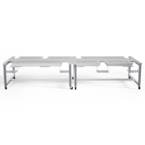
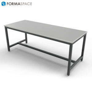
All the furniture within the gowning room is made from stainless steel, including the benches and shoe racks, to make it easier to keep clean. No storage lockers are used (this could trap contaminants); instead, the “bunny suit” gowns that workers wear inside the cleanroom are stored on fixed stainless steel hangers. (Be sure to talk to your Formaspace Design Consultant about these and other furniture elements that we can custom manufacture for you.)
Once inside the gowning room, you begin the process starting at the top, by putting on a bouffant hairnet. If you have a beard, a beard cover goes on at this stage as well. Next, it’s time to put on a facemask, then step your bunny suit, which covers you from head to toe. The final clothing items to put on are the special cleanroom shoes and the booties that cover them.
Mark noted that while the temperature within the cleanroom work environment is held at a comfortable 70 to 72° (to reduce the number of contaminants in the air), bunny suits can still become quite warm inside, due to the combination of wearing both a facemask and a hood. Mark felt that nylon bunny suits are more comfortable temperature-wise than the ones made of Gortex. (Visitors, such as contractors, often wear temporary suits made of Tyvec.)
Now that the bunny suit is on, it’s time to leave the gowning room. Mark explained that many facilities have an intermediate stage at this point: an air shower setup that blows off any small particles before opening the airlock and walking into the cleanroom area proper. (The procedure for exiting cleanroom is simply the reverse, although many facilities don’t require an air shower on the way out.)
Next, we wanted to know about precautions for preventing unwanted ESD (electrostatic discharge) when working in the wafer fab cleanroom facility.
Mark explained that all the furniture used in the cleanroom, such as the chairs, are equipped with metal discharge chains that drag along the perforated floor, ensuring that any electrical charge build-up is kept to a minimum. Workers also need to minimize their buildup of static electricity by wearing a wrist grounding strap (which looks like an old school coiled phone cord) that connects them to ground.
Thanks to Mark Burgholzer
That concludes our discussion with Mark Burgholzer. We’d like to thank him for taking the time to share some of his valuable hands-on insights into the inner workings of cleanrooms inside semiconductor manufacturing facilities.
Formaspace is Your Cleanroom Furniture Partner
Do you need to upgrade or build your next cleanroom project?
Formaspace can help create a custom solution, built just for you at our Austin, Texas factory headquarters.

For example, take a look at this cleanroom furniture project we built a for a space agency that is used to clean and transport rocket parts. It features electro-polished stainless-steel surfaces throughout.

Remember, if you can imagine it, we can build it.
To learn more about these clean projects and to consult with us on your next project, contact your friendly Formaspace Design Consultant today.


